A team of Penn State researchers report that a fabrication technique may offer a path toward mastering the often chaotic flow of heat carriers at the nanoscale in silicon and other semiconductors. The study could be another step toward understanding how to control heat flow through silicon semiconductors and possibly improving the performance of those chips. IMAGE: PENN STATE
Design method may boost semiconductor performance by better handling heat
Posted on June 22, 2020UNIVERSITY PARK, Pa. — Finding ways to manage the flow of heat in silicon could boost the performance of semiconductors, but, so far, discovering the right design has remained elusive. Now, a team of Penn State researchers report that a fabrication technique may offer a path toward mastering the often chaotic flow of heat carriers at the nanoscale in silicon and other semiconductors.
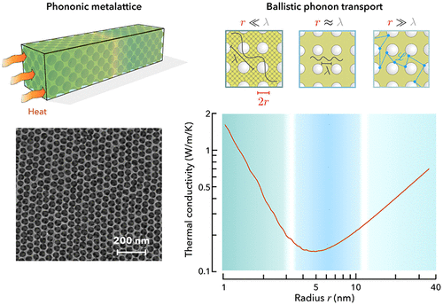
In a study, the researchers used supercomputers to test a design that inserts nanometer-sized holes into a silicon semiconductor and found that the resulting model, which consists of evenly distributed spherical-shaped inclusions could dramatically influence the ability to channel heat via atomic vibrations called phonons. The inclusions are holes with a radii of between 7 to 30 nanometers. As a comparison, a human hair is about 80,000 nanometers wide.
The researchers added that this is a significant step toward understanding how to control heat flow through silicon semiconductors and, one day, improving the performance of those chips.
Controlling the flow of heat is difficult because of the way phonons ricochet throughout materials at certain scales, said Ismaila Dabo, associate professor of materials science and engineering.
“When you look at heat from the level of being made of phonons, the particles that conduct heat, you quickly realize that these phonons can only go so far without being deflected,” said Dabo, who is also an associate of the Institute of Computational and Data Sciences (ICDS), which operates the supercomputer on which the team’s research was conducted. “So, there’s only a limited distance that a phonon can travel in the material and that distance is on the order of 50 nanometers to 1,000 nanometers for most materials.”
When the geometry of the structures made with these materials is on the order of these length scales, the behavior of phonons becomes more complicated, according to Brian Foley, assistant professor of mechanical engineering.
“Over the past few decades people have been trying to engineer lower thermal conductivity materials for things like thermoelectrics and thermal barrier coatings,” said Foley. “This work shows that if you continue this nanostructured-approach into the sub-10 nm regime in an ordered geometric system, you pass through a minimum thermal conductivity and then rapidly recover the bulk properties as the inclusions continue to shrink and ultimately disappear. Now, being able to access the other side of that minimum, I think it is getting more interesting because we can design materials with thermal conductivity that are more sensitive to size parameters.”
While this work represents an important step, it is still just an initial step, according to the researchers, who report their findings in a recent issue of ACS Nano. However, it might open up other possibilities, beyond computer chip enhancements, in the future. The design could, for example, help convert heat that might otherwise be wasted into usable energy.
“This sets up a goal for the next decade or so, I believe, to use advanced systems like these to engineer thermal-equivalents to electrical devices, such as diodes and transistors,” said Foley. “Scavenging heat and helping energy efficiency would be the most direct benefits of these thermal devices — phonon computing and thermal computing are other ways they might be used.”
The researchers said that the work also helps other scientists explore the often weird world of working with phonons. While most people realize that electrons and photons can exhibit both wavelike and particle-like behaviors, they may not know that phonons have a similar quality, said Weinan Chen, graduate research assistant and co-first author of the paper.
“We know that an electron can be either a particle or a wave, which is the foundation of modern physics,” said Chen. “The same concept applies to phonons. It can be seen as a particle and it can be seen as a wave. In this case, it is no longer transporting electricity, it’s a heat current. So, this is very sensitive to temperature and how the temperature is distributed through the material.”
Unlike electrons and photons, phonons need to exist in a condensed matter state — which gives researchers studying phonons a lot of headaches.
“We sometimes think that the electronics-world has it made — with well-defined conducting pathways and weakly-interacting ‘gases’ of electrons and holes that rarely see each other,” said Foley. “But, heat flow can be tougher to study as it is hard to confine and just goes everywhere; not to mention the intricacies of phonons as they bounce into each other, they bounce into other stuff. It’s an interconnected network of cross-talk and collisions; it can be a big a mess.”
Disha Talreja, doctoral student and co-first author of the work, shares this sentiment, saying that measuring heat flow in these complicated structures was very rewarding. Said Talreja, “Synthesizing nanometer sized pores in an ordered fashion in materials like silicon and being able to experimentally capture theoretically predicted diffusion of phonons through them was indeed an exciting journey.”
Dabo and Foley added that the ability to precisely design these nanostructures — or tunability — would not have been possible without nanofabrication techniques developed by the late John Badding.
“The fabrication process, to me, is mind-blowing,” said Foley. “What John Badding developed is disruptive in that it’s a whole new avenue for designing thermal structures. I hope we can help make this part of his legacy to both the chemical and broader sciences.”
Computations for this research were performed on the Roar supercomputer.
The team also included Devon Eichfeld, doctoral student; Shih-Ying Yu, research assistant; Nicolas Poilvert, post-doctoral scholar, all of materials science and engineering; Pratibha Mahale, graduate student; Nabila Nabi Nova, doctoral student; Hiu Yan Cheng, graduate research assistant, and Jennifer L. Russell, graduate student, all in chemistry; G.D. Mahan, distinguished emeritus professor of physics; Suzanne E. Mohney, professor of materials science and engineering; Vincent H. Crespi, distinguished professor of physics, materials science and engineering, and chemistry; Thomas E. Mallouk, Vagelos professor in energy research and professor of chemistry; the late John V. Badding, professor of chemistry; and Venkatraman Gopalan, professor of materials science and engineering and physics.
The National Science Foundation Materials Research Science and Engineering Center for Nanoscale Science supported this research.